Product Summary
The XC3S2000-4FGG676I is a member of Spartan-3 family. The XC3S2000-4FGG676I is a kind of Field-Programmable Gate Array (FPGA) which is specifically designed to meet the needs of high volume, cost-sensitive consumer electronic applications. The XC3S2000-4FGG676I offers densities ranging from 100,000 to 1.6 million system gates. The XC3S2000-4FGG676I builds on the success of the earlier Spartan-IIE family by increasing the amount of logic resources, the capacity of internal RAM, the total number of I/Os, and the overall level of performance as well as by improving clock management functions. The XC3S2000-4FGG676I is a superior alternative to mask programmed ASICs. FPGAs avoid the high initial cost, the lengthy development cycles, and the inherent inflexibility of conventional ASICs. Also, FPGA programmability permits design upgrades in the field with no hardware replacement necessary, an impossibility with ASICs.
Parametrics
XC3S2000-4FGG676I absolute maximum ratings: (1)VCCINT, Internal supply voltage: –0.5 to 1.32 V; (2)VCCAUX, Auxiliary supply voltage: –0.5 to 3.00 V; (3)VCCO, Output driver supply voltage: –0.5 to 3.75 V; (4)VREF, Input reference voltage: –0.5 to VCCO+0.5 V; (5)IIK, Input clamp current per I/O pin,–0.5 V < VIN < (VCCO + 0.5 V): ±100 mA; (6)VESD, Electrostatic Discharge Voltage: Human body model: ±2000 V; (7)Charged device model: ±500 V; Machine model: ±200 V; (8)TJ, Junction temperature: 125℃; (9)TSTG, Storage temperature: –65 to 150℃; (10)TSOL, Soldering Temperature: 220℃.
Features
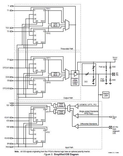
XC3S2000-4FGG676I features: (1)Low-cost, high-performance logic solution for high-volume,consumer-oriented applications: Densities up to 74,880 logic cells; (2)SelectIOinterface signaling: Up to 633 I/O pins; 622+ Mb/s data transfer rate per I/O; 18 single-ended signal standards; 8 differential I/O standards including LVDS, RSDS; Termination by Digitally Controlled Impedance; Signal swing ranging from 1.14V to 3.465V; Double Data Rate (DDR) support; DDR, DDR2 SDRAM support up to 333 Mbps; (3)Logic resources: Abundant logic cells with shift register capability; Wide, fast multiplexers; Fast look-ahead carry logic; Dedicated 18 x 18 multipliers; JTAG logic compatible with IEEE 1149.1/1532; (4)SelectRAMhierarchical memory: Up to 1,872 Kbits of total block RAM; Up to 520 Kbits of total distributed RAM; (5)Digital Clock Manager (up to four DCMs): Clock skew elimination; Frequency synthesis; High resolution phase shifting; (6)Eight global clock lines and abundant routing; (7)Fully supported by Xilinx ISEand WebPACK software development systems; (8)MicroBlazeand PicoBlazeprocessor, PCI PCI ExpressPIPE Endpoint, and other IP cores; (9)Pb-free packaging options; (10)Automotive Spartan-3 XA Family variant.
Diagrams

| Image | Part No | Mfg | Description |  |
Pricing (USD) |
Quantity | ||||||||||
|---|---|---|---|---|---|---|---|---|---|---|---|---|---|---|---|---|
 |
 XC3S2000-4FGG676I |
 |
 SPARTAN-3A FPGA 2M STD 676-FBGA |
 Data Sheet |

|
|
||||||||||
| Image | Part No | Mfg | Description |  |
Pricing (USD) |
Quantity | ||||||||||
 |
 XC3S1000 |
 Other |
 |
 Data Sheet |
 Negotiable |
|
||||||||||
 |
 XC3S1000-4FG456I |
 |
 IC FPGA SPARTAN 3 456FBGA |
 Data Sheet |

|
|
||||||||||
 |
 XC3S1000-4FG676I |
 |
 IC FPGA SPARTAN 3 676FBGA |
 Data Sheet |

|
|
||||||||||
 |
 XC3S1000-4FGG320C |
 |
 SPARTAN-3A FPGA 1M STD 320-FBGA |
 Data Sheet |

|
|
||||||||||
 |
 XC3S1000-4FGG320I |
 |
 IC SPARTAN-3A FPGA 1M 320-FBGA |
 Data Sheet |

|
|
||||||||||
 |
 XC3S1000-4FGG456C |
 |
 IC SPARTAN-3 FPGA 1M 456-FBGA |
 Data Sheet |

|
|
||||||||||
 (China (Mainland))


